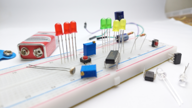
If you’ve been playing around with breadboards and jumper wires for a while, there comes a point where everything starts to look like a messy bowl of noodles. That’s usually the moment you think:
“I wish I could make this into a proper, professional-looking circuit.”
That’s where PCB design comes in.
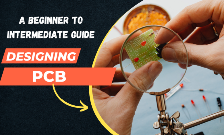
A PCB (Printed Circuit Board) lets you turn your idea into a neat, compact, and reliable hardware design that you can actually hold in your hand.
If you’re new to this, don’t worry this guide walks you through the PCB design process in a simple, practical way.
What Exactly Is a PCB?
Think of a PCB as the “final version” of your circuit.
All those wires you manually connect on a breadboard are replaced by thin copper tracks. Components sit neatly on fixed pads, and everything stays exactly where it should be permanently.
If you plan to make a robot, IoT device, smart plant monitor, or even a simple LED based project, PCB design is the skill that upgrades your project from “prototype” to “product.”
Tools You’ll Need
To design a PCB, you don’t need expensive software.
Here are tools real beginners actually use
- EasyEDA – Very beginner-friendly, works in your browser
- KiCad – Free and more advanced, good for long-term learning
- Eagle – Popular with makers
- Altium – Professional tool (you don’t need this yet)
If you’re unsure where to start:
- Use EasyEDA if you’re a beginner
- Use KiCad if you want more control and plan to go deeper
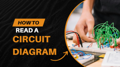
Step 1 – Draw the Schematic
The schematic is basically the “map” of your circuit.
This is where you place symbols for resistors, chips, sensors, etc., and connect them logically.
A few human-friendly tips:
- Keep your schematic tidy (future you will thank past you)
- Double-check polarities (diodes, LEDs, electrolytic capacitors)
- Label your signals so you don’t get confused later
- Use proper values — don’t leave “R1 = 0 Ω??” by mistake
Once your schematic looks clean and complete, you can move to the fun part: the layout.
Step 2 – Switching to the PCB Layout
This is where things get interesting.
Your software will take your schematic and let you place actual component footprints on a board.
Your job here
- Decide the board size
- Place components on it
- Route the tracks
- Add labels or text
- Make it manufacturable
Beginners often feel overwhelmed the first time – but trust me, after 2 to 3 boards, this becomes surprisingly enjoyable.
Step 3 – Component Placement (The Unsung Hero Step)
Good PCB designers always say
“90% of PCB design is component placement. Routing is the easy part.”
Here’s the trick
- Put related components close together
- Don’t scatter things randomly
- Keep the power section grouped
- Place connectors near edges
- Keep sensors away from heat sources
- Put decoupling capacitors as close as possible to IC pins
If your placement is neat, routing becomes almost effortless.
Step 4 – Routing the Tracks
Routing is the process of drawing copper paths between parts.
Some friendly advice
- Use 45° angles – they look nicer
- Don’t make power traces thin
- Keep noisy signals away from sensitive analog ones
- Use vias only when needed
- Avoid crossing tracks if possible
- Don’t overthink – you can always undo and try again
Beginners often try to make routes “pretty.”
Instead, focus on making them clean, short, and functional.
Step 5 – Add a Ground Plane
One of the simplest ways to instantly improve your PCB is to add a ground plane.
It helps with
- Reducing noise
- Better signal stability
- Cleaner routing
- Better performance with sensors
Most design tools let you add a ground plane with one click. Always do it.
Step 6 – Run a Design Rule Check (DRC)
Before ordering your board, run the DRC.
It will warn you about:
- Tracks that are too close
- Components overlapping
- Unconnected nets
- Wrong footprints
- Clearance issues
Fix everything until you get a clean report.
This step saves you from expensive mistakes.
Step 7 – Export the Gerber Files and Order the PCB
Gerber files are like the “PDF version” of your PCB design manufacturers need them to build your board.
Popular manufacturers:
- JLCPCB
- PCBWay
- Seeed Fusion
- OSH Park
Most people order 5 PCBs just to test.
It usually costs around $2–$10 for basic boards.
Common Beginner Mistakes (Everyone Does These)
Here are the mistakes almost all DIY designers make at some point:
- Wrong footprint for a component
- Tracks too thin for the actual current
- Forgetting ground connections
- Missing mounting holes
- Components placed too close
- No labels on the silkscreen
- Power polarity reversed (ouch)
Don’t worry — everyone learns PCB design through small mistakes.
Going from Beginner to Intermediate
Once you’re comfortable with basic designs, try exploring:
- 2 layer and 4 layer PCBs
- Differential pairs
- Controlled impedance routing
- RF design basics
- Thermal relief and heat spreading
- EMC/EMI considerations
These skills slowly move you towards professional-level PCB design.
Final Thoughts
Designing a PCB is one of those skills that look complicated from the outside, but once you start, it becomes one of the most satisfying parts of electronics.
The first time you hold your own PCB – your design, your idea, turned into something real — it’s honestly a great feeling.
This is all about Designing a PCB, Thanks for reading.
Check out my other articles.